Tiedosto:Wafer flats convention v2.svg

Alkuperäinen tiedosto (SVG-tiedosto; oletustarkkuus 150 × 150 kuvapistettä; tiedostokoko 13 KiB)
| Tämä tiedosto on tiedostotietokanta Wikimedia Commonsista. Tiedot kuvaussivulta näkyvät alla. |  |
Tiedoston kuvaussivu Commonsissa |
Yhteenveto
| Kuvaus |
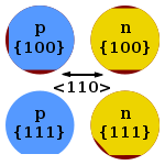
Wafer flats convention, based on Image:Wafer flats convention.PNG Conventional meaning of flats in semiconductor wafers. Red denotes material that has been removed. Wafer orientation is the orientation of the crystallographic plane in which the crystal grew. Wafer type indicated the type of doping.
|
| Päiväys | |
| Lähde |
self-made, Tämä vektorigrafiikkatiedosto luotiin käyttäen apuna ohjelmaa Inkscape . |
| Tekijä | Twisp |
| Muut versiot | Wafer flats convention.PNG |
Lisenssi
| Minä, tämän teoksen tekijänoikeudellinen omistaja, julkaisen tämän teoksen public domainiin eli luovun kaikista tekijänoikeuksista lain sallimissa puitteissa. Tämä on voimassa maailmanlaajuisesti. Joissain maissa laki ei mahdollista tätä. Mikäli näin on: Myönnän kenelle tahansa oikeuden käyttää tätä teosta mihin tahansa tarkoitukseen, ilman mitään ehtoja, ellei laki vaadi ehtojen asettamista. |
Tiedoston historia
Päiväystä napsauttamalla näet, millainen tiedosto oli kyseisellä hetkellä.
| Päiväys | Pienoiskuva | Koko | Käyttäjä | Kommentti | |
|---|---|---|---|---|---|
| nykyinen | 25. syyskuuta 2013 kello 00.40 | | 150 × 150 (13 KiB) | Cepheiden | fixed position of secondary flat Silicon processing for the VLSI era - Vol. 1 - Process technology; S Wolf; RN Tauber - Lattice Press; 1986; ISBN 096167237; p. 23 |
| 23. joulukuuta 2008 kello 03.37 |  | 150 × 150 (13 KiB) | Inductiveload | Added arrow indication <110> direction and enlarged flats so they can be easily seen | |
| 1. maaliskuuta 2008 kello 00.17 |  | 150 × 150 (9 KiB) | Twisp | ||
| 1. maaliskuuta 2008 kello 00.13 |  | 150 × 150 (9 KiB) | Twisp | ||
| 1. maaliskuuta 2008 kello 00.06 |  | 150 × 150 (8 KiB) | Twisp | ||
| 29. helmikuuta 2008 kello 23.59 |  | 150 × 150 (8 KiB) | Twisp | ||
| 29. helmikuuta 2008 kello 21.09 |  | 150 × 150 (9 KiB) | Twisp | {{Information |Description= Wafer flats convention, based on Image:Wafer flats convention.PNG Conventional meaning of ''flats'' in semiconductor wafers. Black denotes material that has been removed. Wafer orientation is |
Tiedoston käyttö
Seuraava sivu käyttää tätä tiedostoa:
Tiedoston järjestelmänlaajuinen käyttö
Seuraavat muut wikit käyttävät tätä tiedostoa:
- Käyttö kohteessa ca.wikipedia.org
- Käyttö kohteessa cs.wikipedia.org
- Käyttö kohteessa de.wikipedia.org
- Käyttö kohteessa en.wikipedia.org
- Käyttö kohteessa es.wikipedia.org
- Käyttö kohteessa et.wikipedia.org
- Käyttö kohteessa eu.wikipedia.org
- Käyttö kohteessa it.wikipedia.org
- Käyttö kohteessa it.wikibooks.org
- Käyttö kohteessa ja.wikipedia.org
- Käyttö kohteessa ko.wikipedia.org
- Käyttö kohteessa nl.wikipedia.org
- Käyttö kohteessa pl.wikipedia.org
- Käyttö kohteessa ro.wikipedia.org
- Käyttö kohteessa sk.wikipedia.org
- Käyttö kohteessa uk.wikipedia.org
- Käyttö kohteessa www.wikidata.org