Tiedosto:Cmos-chip structure in 2000s (en).svg

Alkuperäinen tiedosto (SVG-tiedosto; oletustarkkuus 550 × 810 kuvapistettä; tiedostokoko 138 KiB)
| Tämä tiedosto on tiedostotietokanta Wikimedia Commonsista. Tiedot kuvaussivulta näkyvät alla. | .svg?uselang=fi) |
Tiedoston kuvaussivu Commonsissa |
Yhteenveto
| Kuvaus |
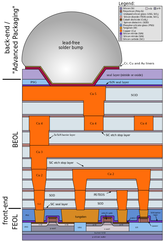
Català: Estructura esquemàtica d'un xip CMOS, tal com es va construir a principis dels anys 2000. El gràfic mostra els LDD-MISFET sobre un substrat de silici SOI amb cinc capes de metal·lització i un tap de soldadura per a la unió de xip. També mostra la secció per a FEOL (front-end de línia), BEOL (back-end de línia) i les primeres parts del procés de back-end. (versió traduïda a l'alemany)
English: Schematic structure of a CMOS chip, like it is built in the early 2000s. The graphic shows LDD-MISFET's on a SOI silicon substrate with five metallization layers and solder bump for flip-chip bonding. Also it shows the section for FEOL (front-end of line), BEOL (back-end of line) and first parts of back-end process. (translated German version) |
| Päiväys | 9. joulukuuta 2006 (tallennuspäivä) |
| Lähde | self made (from university scripts and scientific papers) |
| Tekijä | Cepheiden |
| Muut versiot |
Other related versions:[]
|
.svg&lang=ca)
.svg&lang=en)

.svg)
.svg)
|
Tässä SVG-tiedostossa on tekstiä, jonka voi kääntää helposti suomen kielelle käyttäen SVG-editoria kuten Inkscapea tai Adobe Illustratoria. Lisätietoja on sivulla Commons:Translation possible/Learn more. Voit myös ladata ja tallentaa sen, ja kääntää sen manuaalisesti tekstimuokkaimella. |
Tämä tiedosto on käännetty SVG Upottaaksesi tämän tiedoston omalla kielelläsi (mikäli saatavilla) käytä Kääntääksesi tämän tiedoston omalle kielellesi lataa tiedosto tietokoneellesi, lisää käännöksesi ja lataa se uudelleen samalla nimellä. Mikäli et ole varma miten tämä tehdään, saat apua sivulta Graphics Lab. |
Lisenssi

|
Voit kopioida, levittää ja/tai muuttaa tätä asiakirjaa GNU Free Documentation License -lisenssin version 1.2 tai minkä tahansa Free Software Foundationin julkaiseman myöhemmän version ehtojen alaisena; ei koske muuttumattomia kohtia, etukannen tekstejä eikä takakannen tekstejä. Kopio tästä lisenssistä on saatavilla osiossa GNU Free Documentation License. |
| Tämä tiedosto on lisensoitu Creative Commons Nimeä-JaaSamoin 3.0 Ei sovitettu -lisenssillä. | ||
| ||
| Lisensointimerkintä lisätiin tähän tiedostoon osana GFDL-lisensointipäivitystä. |
- Voit:
- jakaa – kopioida, levittää ja esittää teosta
- remiksata – valmistaa muutettuja teoksia
- Seuraavilla ehdoilla:
- nimeäminen – Sinun on mainittava lähde asianmukaisesti, tarjottava linkki lisenssiin sekä merkittävä, mikäli olet tehnyt muutoksia. Voit tehdä yllä olevan millä tahansa kohtuullisella tavalla, mutta et siten, että annat ymmärtää lisenssinantajan suosittelevan sinua tai teoksen käyttöäsi.
Tiedoston historia
Päiväystä napsauttamalla näet, millainen tiedosto oli kyseisellä hetkellä.
| Päiväys | Pienoiskuva | Koko | Käyttäjä | Kommentti | |
|---|---|---|---|---|---|
| nykyinen | 5. helmikuuta 2024 kello 17.35 | | 550 × 810 (138 KiB) | Manlleus | File uploaded using svgtranslate tool (https://svgtranslate.toolforge.org/). Added translation for ca. |
| 5. helmikuuta 2024 kello 17.25 |  | 550 × 810 (97 KiB) | Manlleus | fixed text labels for translation | |
| 9. joulukuuta 2006 kello 21.52 |  | 550 × 810 (85 KiB) | Cepheiden | {{Information |Description= Schematic structure of a CMOS chip, like it is build in the early 2000s. The grafic shows LDD-MISFET's on a SOI silicon substrate with five metallization layers and solder bump for flip-chip bonding. Also it shows the section f | |
| 9. joulukuuta 2006 kello 21.49 |  | 550 × 810 (85 KiB) | Cepheiden | {{Information |Description= Schematic structure of a CMOS chip, like it is build in the early 2000s. The grafic shows LDD-MISFET's on a SOI silicon substrate with five metallization layers and solder bumb for flip-chip bonding. Also it shows the section f |
Tiedoston käyttö
Seuraavat 3 sivua käyttävät tätä tiedostoa:
Tiedoston järjestelmänlaajuinen käyttö
Seuraavat muut wikit käyttävät tätä tiedostoa:
- Käyttö kohteessa ar.wikipedia.org
- Käyttö kohteessa ca.wikipedia.org
- Käyttö kohteessa en.wikipedia.org
- Käyttö kohteessa fa.wikipedia.org
- Käyttö kohteessa hy.wikipedia.org
- Käyttö kohteessa ja.wikipedia.org
- Käyttö kohteessa ko.wikipedia.org
- Käyttö kohteessa zh.wikipedia.org
.svg)